
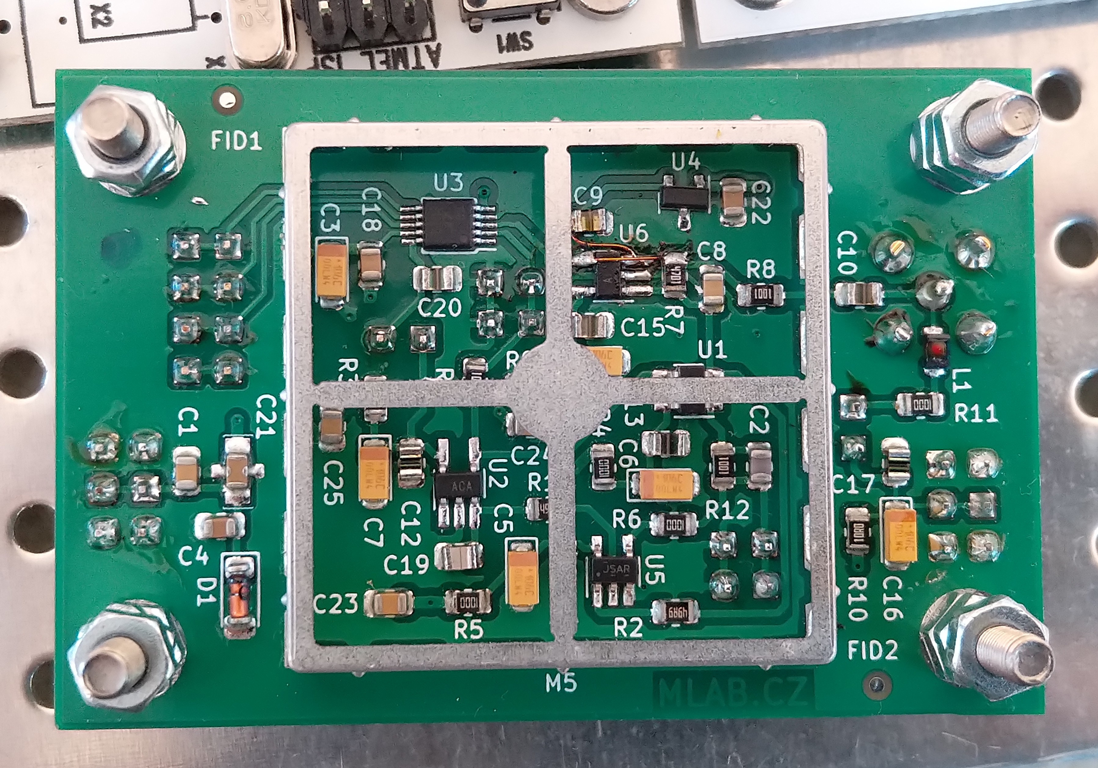
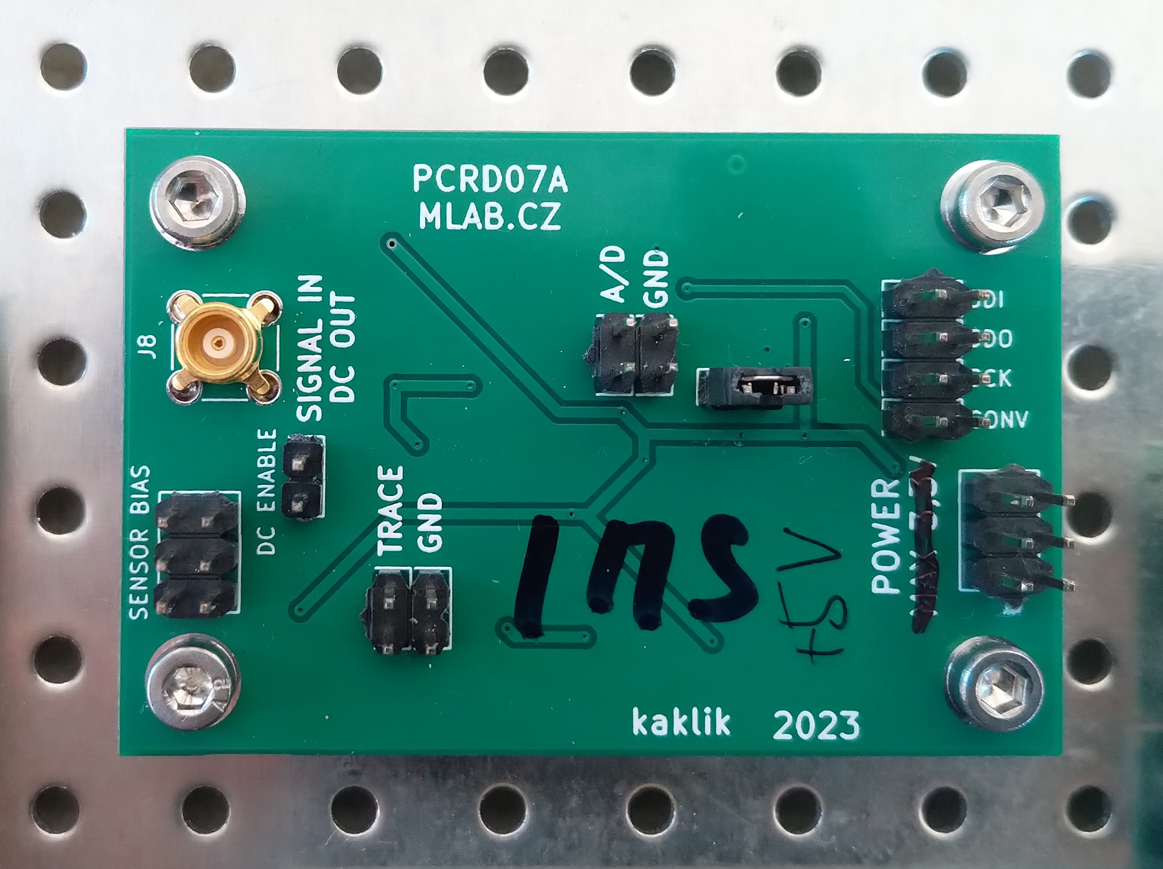
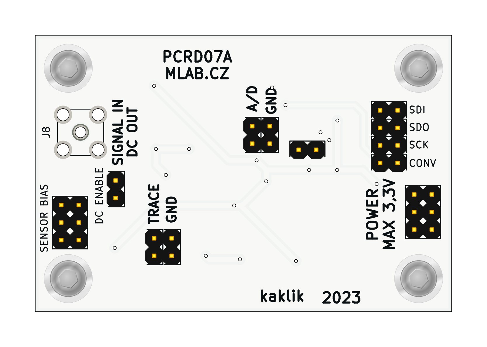


The analog backend for radiation detector with pulsed outputs. The pulses are expected to carry information about energy and the type of particle interacting with the detector. The detectors could be semiconductor diodes or scintillators with semiconductor photomultipliers.


Examples of detectors that could be connected to the PCRD07 analog-backend.
The circuit can operate in multiple modes. The operation mode depends on the logic used to control the circuit.
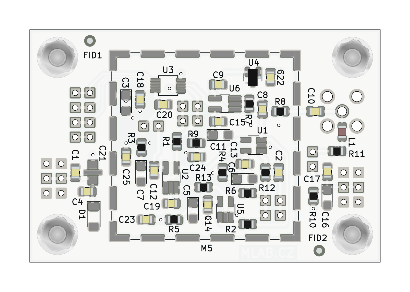
The signal output from the scintillation detector is pulsed. The pulses are stored in a specially developed sample-hold circuit that behaves as a signal follower and analog memory. When signal #PeakDetect_Trace is in H an analog switch U5 turns on and a signal at an output U2 follows a signal at the input with a slight delay which is done by R13 and C19. If signal #PeakDetect_Trace is switched to a high impedance state the analog switch U5 starts to be controlled by a comparator U1. In this case, when the input signal goes from high to low, a positive input of the comparator will be at a higher voltage than a negative input, following a voltage at capacitor C19.

It causes the switching-off of the analog switch U5 and the capacitor C19 holds its last voltage value. This behavior is similar to a peak detector circuit. In the next step, the stored voltage can be converted by ADC connected at the output and after this conversion, the input #PeakDetect_Trace goes again to H and the circuit changes behavior to signal follower circuit. The described sample-hold circuit does not suffer from typical peak detector circuit ills like insensitivity to small signals, mistreatment of negative signals, or discharging the capacitor by leakage current through diodes.
Moreover, this circuit can be used as a pulse discriminator as well. The signal #PeakDetect_Trace can be connected to an input of digital circuits when it is controlled by the comparator U1. When the input signal goes from high to low, the signal #PeakDetect_Trace goes from high to low as well. This behavior can be used for the detection of the falling edge of the signal. There is only one constraint of this circuit, the input signal can not change raising/falling time widely and the RC time constant (R13, C19) must be chosen correctly, respecting the input signal time properties.
More details about the principle are in DOCTORAL THESIS, Research on cosmic rays on board aircraft using a newly developed PIN diode detector, 2020, CTU in Prague