MPC17529HB01 - Dual H‑Bridge
Dual H‑Bridge 2.0–6.8 V / 2×0.7 A (peak 2×1.4 A) with Freescale MPC17529
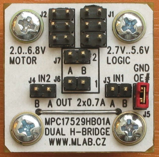
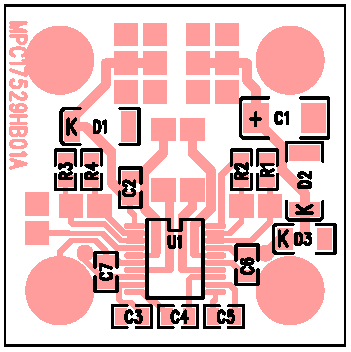
| Top view |
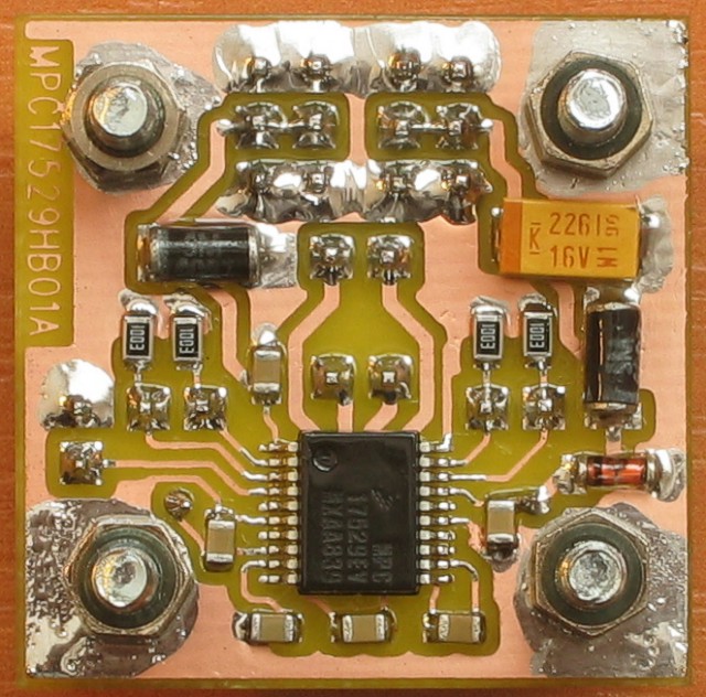
Bottom view |
 |
 |
Features
- Dual H‑bridge motor driver based on Freescale MPC17529
- Separate motor (VM) and logic (VDD) supplies
- Motor supply: 2.0–6.8 V (absolute max. 8.0 V)
- Logic supply: 2.7–5.7 V (absolute max. 7.0 V)
- Continuous output current: 2×0.7 A; peak: 2×1.4 A
- Typical bridge ON resistance: \~0.7 Ω
- Logic supply current: up to 3 mA
- PWM control up to 200 kHz (static operation allowed)
- On‑board reverse‑polarity protection for both supplies; VM clamp by 8.2 V Zener
- MLAB 30 × 30 × 15 mm form factor with M3 mounting
Electrical characteristics (summary)
- VM (motor power): 2.0–6.8 V (abs. max 8.0 V)
- VDD (logic power): 2.7–5.7 V (abs. max 7.0 V)
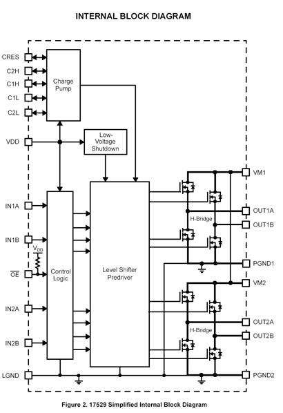
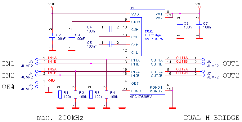
- Outputs: two independent H‑bridges: OUT1A/OUT1B and OUT2A/OUT2B
- Control inputs: IN1A, IN1B, IN2A, IN2B (CMOS/TTL compatible to VDD)
- Global enable: OE# (active‑low, shared by both bridges)
- Grounds: LGND (logic), PGND1/PGND2 (power); star‑connect at the module
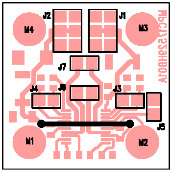
Connectors & signals
Silk‑labeled headers provide access to all signals:
-
Power
-
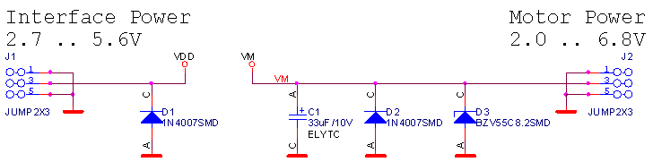
J1 – Interface Power (VDD, LGND): 2×3 header
- J2 – Motor Power (VM, PGND): 2×3 header, reverse‑polarity protected; VM clamped by Zener
-
Control
-
OE# (active‑low enable, common for both channels)
- IN1A, IN1B, IN2A, IN2B (per‑channel direction/PWM inputs)
-
Outputs
-
OUT1A, OUT1B (Channel 1)
- OUT2A, OUT2B (Channel 2)
PWM can be applied to OE# or to the respective INx input. Keep PWM ≤ 200 kHz.
Control logic (per channel)
For either channel x (1 or 2):
| OE# |
INxA |
INxB |
OUTxA |
OUTxB |
Function |
| H |
X |
X |
Z |
Z |
Outputs disabled (Hi‑Z) |
| L |
L |
L |
L |
L |
Brake (both low) |
| L |
L |
H |
H |
L |
Drive – direction A→B |
| L |
H |
L |
L |
H |
Drive – direction B→A |
| L |
H |
H |
Z |
Z |
Coast (Hi‑Z) |
Power & layout recommendations
- Decouple VDD and VM close to the module (≥ 100 nF each); keep C1 (bulk on VM) near the connector.
- Keep motor current paths short and wide; route power returns to PGND; tie LGND to PGND at the module.
- When sharing a source with logic, insert an LC (preferred) or RC filter and a regulator toward the controller.
Motor EMI suppression
Commutator motors generate significant EMI. To avoid MCU resets and erratic behavior:
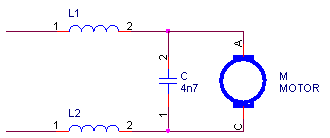
- Solder a 4.7 nF ceramic capacitor directly across the motor terminals.
- If needed, add series chokes (a few turns on a ferrite core) in both motor leads.
- For harsh environments, power logic from a separate source or via a filtered/regulated branch.
Protection circuitry on board
- D1, D2: reverse‑polarity protection diodes on VM and VDD inputs
- D3 (≈ 8.2 V Zener): clamps VM when the motor is back‑driven with supply disconnected
- C1 (33 µF) and C2–C7 (100 nF): bulk and local decoupling
Mechanical
- PCB 30 × 30 mm, overall height ≈ 15 mm above base
- Four M3 mounting holes; typical hardware: M3×12 screws, M3 washers, M3×5 standoffs
Assembly notes
- SMD parts are on the bottom side; top side carries headers, screws, and one wire link.
- Solder the MPC17529 IC first; use minimal solder and suitable SMD flux.
- Observe polarity/orientation of D1/D2 (1N4007 SMD, MELF), D3 (BZV55C8V2, MiniMELF), and C1 (electrolytic).
- After power‑up (VM ≈ 5 V), verify operation with a small DC motor using the control truth table above.
Typical use
- Provide VM from a 2.0–6.8 V battery pack (e.g., 4×Ni‑MH or 1×Li‑ion).
- Provide VDD from a 2.7–5.7 V source/regulator.
- Connect MCU GPIOs to IN1A/IN1B/IN2A/IN2B; drive OE# low to enable.
- Apply PWM to INx (or OE#) for speed control; reverse by swapping INxA/INxB logic levels.
- Add a 4.7 nF capacitor at the motor and, if necessary, series chokes to mitigate EMI.