Module MPC17511HB01 was replaced by newer version. Look at HBRIDGE03.
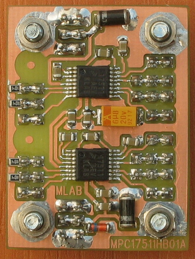
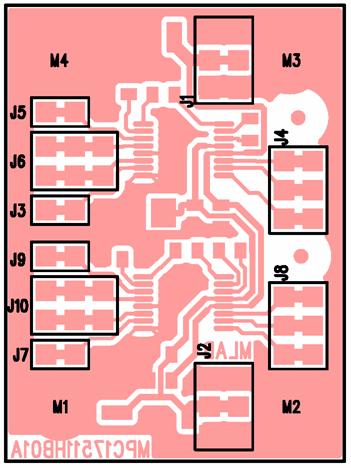
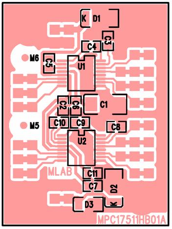


H‑Bridge motor driver module (2×) using NXP/Freescale MPC17511A.


INx or ENx)| Parameter | Value | Notes |
|---|---|---|
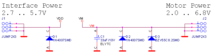
| Motor supply (VM) | 2.0 – 6.8 V | Absolute max 8.0 V |
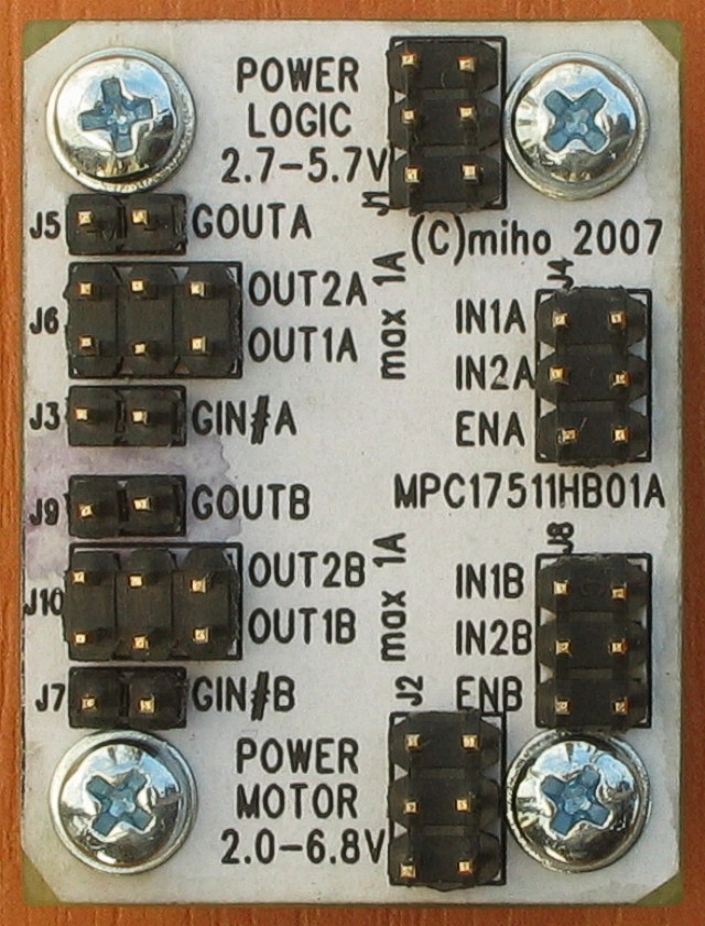
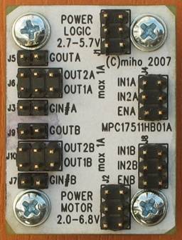
| Logic supply (VDD) | 2.7 – 5.7 V | Absolute max 7.0 V |
| Output current (per bridge) | 1 A continuous | Up to 3 A peak |
| HS+LS on‑resistance | \~0.45 Ω typ. | Per bridge path |
| Logic current | ≤ 3 mA | No load |
| PWM frequency | 0 – 200 kHz | DC (static) operation allowed |
| Module size (W×D×H) | 40 × 30 × 15 mm | Height over base |
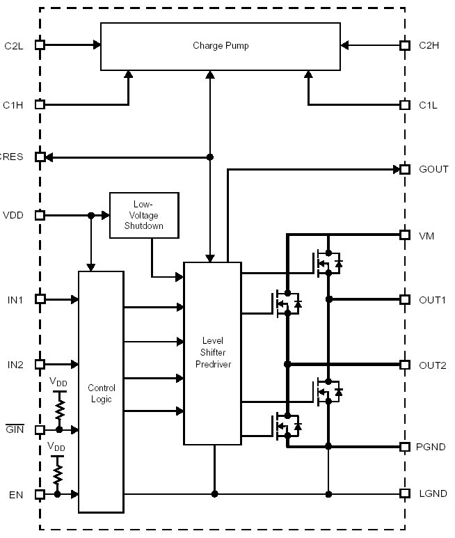
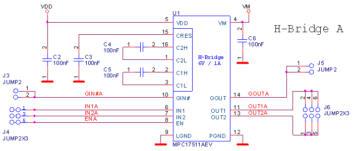
Each bridge (A/B) exposes the following signals.
VM — Motor supply input (2.0–6.8 V)VDD — Logic supply input (2.7–5.7 V)PGND, LGND — Power/logic grounds (tie at the module)OUT1x, OUT2x — Motor outputs (channel x = A/B)IN1x, IN2x — Direction inputsENx — Enable input (can be PWM’d)GIN#, GOUT — Gate‑drive I/O for an optional external high‑side N‑FET (not populated on the module)Note: The IC separates VM and VDD, allowing direct battery drive for the motor while powering the controller from a regulated VDD.
ENx = H, IN1x = H, IN2x = L → Forward (OUT1x = H, OUT2x = L)ENx = H, IN1x = L, IN2x = H → Reverse (OUT1x = L, OUT2x = H)ENx = H, IN1x = H, IN2x = H → Brake (low‑side conduction)ENx = H, IN1x = L, IN2x = L → Coast (outputs off/high‑Z)ENx = L → Bridge disabled / low‑powerRefer to the MPC17511A datasheet for the complete truth table and timing.
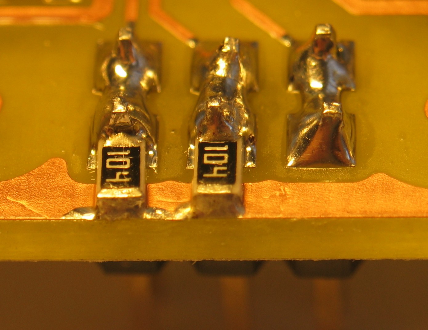
IN1x/IN2x. To prevent a floating state at power‑up, populate 100 kΩ pull‑downs from each IN1x and IN2x to GND (four resistors total across both bridges).IN1x/IN2x/ENx per the functional summary and verify motor direction and braking.INx or EN as required by your control strategy.